The introduction of the Tau Scaling Law by He Tingbo is a shift in chip development, as traditional scaling methods like Moore's Law start to wane. This new framework from Huawei aims to redefine how the company, and possibly the entire industry, will manage the complexities of semiconductor advancement in the years ahead.
He Tingbo, often called Huawei's 'chip queen', has emerged as a key figure in China's technology narrative. Her insights into chip innovation are not just theoretical; they represent a strategic shift for Huawei as it strives to maintain its competitive edge in a fast-changing market. The Tau Scaling Law offers a fresh methodology for enhancing chip performance, moving beyond the historical benchmarks set by Moore's Law, which is increasingly showing signs of slowing.
The Context of Moore's Law
For decades, Moore's Law has served as the cornerstone of semiconductor development, predicting that the number of transistors on a chip would double roughly every two years. This prediction has fueled relentless innovation, resulting in exponential growth in computing power. However, as the physical limitations of silicon technology become more evident, the industry faces a tipping point where such exponential growth may no longer be achievable.
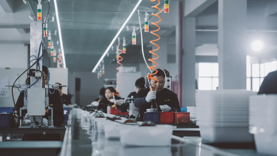
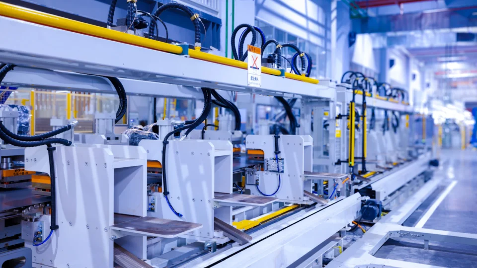
He Tingbo's Tau Scaling Law seeks to tackle this looming challenge by proposing alternative strategies for chip design and architecture. While specific details of the Tau Scaling Law remain confidential, industry experts suggest it could involve innovative approaches to chip materials, architecture, and power efficiency. This could lead to significant advancements in AI infrastructure and GPU networks, areas where Huawei is particularly focused.
Implications for AI Infrastructure and GPU Networks
The implications of the Tau Scaling Law reach beyond Huawei's immediate operations. As AI technologies demand increasingly powerful hardware, the urgency for efficient chip development has never been greater. With this new framework, Huawei could establish itself as a leader in providing the necessary infrastructure for AI applications, potentially influencing various sectors, including autonomous vehicles, cloud computing, and smart devices.
as companies globally confront the limitations imposed by Moore's Law, He Tingbo's contributions might inspire a wider shift in the semiconductor industry. If successful, the Tau Scaling Law could encourage other tech giants to explore alternative methodologies, sparking a wave of innovation that aligns with modern computing needs.
Looking Ahead
As Huawei prepares to roll out the Tau Scaling Law, the next few years will be key for both the company and the semiconductor industry. He Tingbo's leadership in this initiative is likely to shape the future of chip development, with potential ripple effects across the global tech landscape. The transition from traditional scaling laws to innovative frameworks could herald a new chapter in semiconductor design, paving the way for advancements critical in an AI-driven world.
He Tingbo's Tau Scaling Law signifies not just a change in Huawei's strategy, but a potential roadmap for the future of chip development amid the challenges presented by Moore's Law. The tech community will be closely monitoring these developments, eager to see their impact on AI infrastructure and GPU networks across various industries.