A strategic partnership between ASML and Tata Electronics is set to propel India into the forefront of semiconductor manufacturing, with the establishment of the country's first commercial 300-mm fab in Dholera, Gujarat. This $11 billion facility is projected to produce 50,000 wafers monthly, meeting the rising demands of automotive, mobile devices, and AI applications.
The recently announced Memorandum of Understanding (MoU) details ASML's commitment to supply advanced lithography equipment and technical expertise, essential for the timely development of this ambitious project. Randhir Thakur, CEO of Tata Electronics, noted, “ASML’s deep expertise in holistic lithography solutions will ensure the timely ramp of our fab in Dholera, create a resilient and trusted supply chain for our global customers.”
Implications for India's Semiconductor Landscape
As India aims to strengthen its semiconductor capabilities, the partnership goes beyond just providing equipment. It includes workforce training, supply chain development, and research infrastructure, highlighting a thorough approach to building a sustainable semiconductor ecosystem. Christophe Fouquet, ASML's president and CEO, pointed out the country's growing semiconductor sector, calling it a source of “compelling opportunities.”
The Dholera fab will produce a variety of semiconductors, including high-performance logic chips and radio-frequency-enabled SoCs for Bluetooth and Wi-Fi applications. The technology nodes will range from 28 nm to 110 nm, targeting a lucrative market segment currently generating around $40 billion annually, with projections suggesting growth to $60 billion when considering integrated device manufacturers.
Construction and Future Prospects
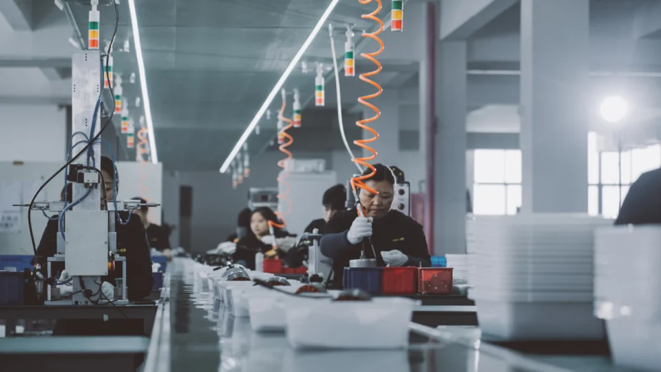
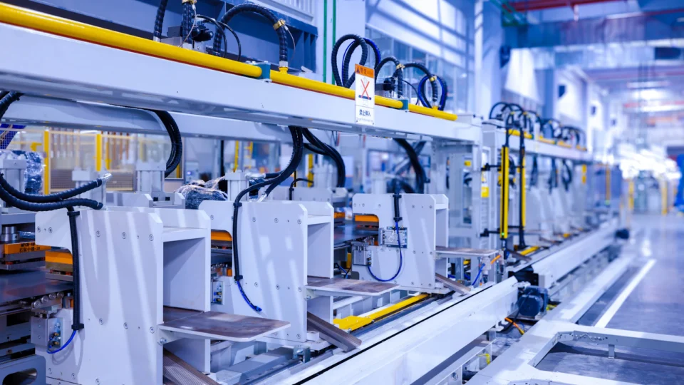
Construction is actively underway on the 160-acre site, with about 1,500 workers involved in what is expected to be a fully automated, “lights-out” Industry 4.0 facility. The project is scheduled to begin operations in 2027. Tata Electronics has also formed partnerships with notable companies, including Taiwan’s Powerchip Semiconductor Manufacturing Corporation and Tokyo Electron, to enhance its technological capabilities.
The anticipated growth in semiconductor consumption in India—from about $34 billion to approximately $110 billion over the next eight years—highlights the urgency and importance of this initiative. This surge is driven by increasing demands in the wireless, consumer electronics, and automotive sectors, marking a pivotal moment for India's role in the global chip supply chain.
Strengthening Global Semiconductor Cooperation
This collaboration not only boosts India's self-sufficiency in semiconductor manufacturing but also strengthens technological ties between India and the Netherlands. As both countries work to enhance their positions in the global semiconductor supply chain, the ASML-Tata partnership represents a significant step towards achieving greater autonomy in chip production. With established agreements and a clear development roadmap, the future of India's semiconductor landscape looks promising, positioning it as a key player in the global market.
Quick answers
What is the capacity of the new semiconductor fab in Dholera?
The facility is expected to produce 50,000 wafers per month.
What technology nodes will the Dholera fab utilize?
The fab will manufacture semiconductors using technology nodes ranging from 28 nm to 110 nm.
When is the Dholera semiconductor fab expected to become operational?
The facility is planned to be operational by 2027.
What are the expected trends in semiconductor consumption in India?
India's semiconductor consumption is projected to triple from approximately $34 billion to around $110 billion over the next eight years.